ISSCC - SAN FRANCISCO, Calif. - February 7, 2006
- Elpida Memory, Inc. (Elpida), Japan's leading global supplier of
Dynamic Random Access Memory (DRAM), today announced the development of
new high-speed, low-power circuit technologies for DDR3 SDRAM in a
paper presented at the International Solid State Circuits Conference
(ISSCC). The new technologies consist of a transfer circuit that
realizes high-speed access time (data readout time), and a data readout
timing generator that enables stable high-speed data transfer rate in
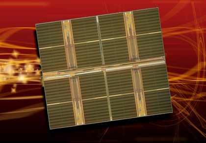
the DRAM's output block. Using the new technologies, Elpida produced a
512 Megabit DDR3 SDRAM with a column access time of 8.75 ns and data
transfer rate of 1.6 Gigabits per second (Gbps). This is an ultra-fast
next-generation DRAM for the high-end server and computing markets.
With
the dramatic rise in processor clock frequencies, DRAM must deliver an
even faster operating performance without sacrificing power efficiency.
Following the standardization of high-speed DDR1 and DDR2 SDRAM, the
DDR3 SDRAM specification is now in the process of being standardized.
DDR3 effectively doubles the performance of the DDR2 architecture and
is expected to become the next-generation DRAM that realizes high-speed
data readout and high-speed data transfer while operating at a mere 1.5
V.
In developing next-generation 512 Megabit
DDR3 SDRAM, Elpida wanted to provide high-end DRAM customers with
circuit technologies that would deliver a faster access time and a
faster data transfer rate than any other product. Elpida found that the
data readout speed could be increased by blanket-reading data from the
DRAM's memory array and transferring that data to the output circuit
using time division, thus cutting down on the number of data signal
lines required and reducing the parasitic capacitance. The company also
devised a technology that would enable high-speed data transfer by
developing counters that could control generation of the data readout
timing on a clock with double the cycle time of DDR2 while still
providing enough operating margin.
Newly Developed Technologies
- Time-division transfer of blanket-read data in the memory array:
With the basic DDR3 system, eight bits of data are blanket read
simultaneously from the DRAM's memory array, enabling data to be read
by the peripheral circuits eight times faster than the speed of data
readout in the array. By executing at different times (time division)
to split the transfer of data from the array to the output buffer
circuit into two operations, the number of signal lines can be halved,
enabling the expansion of the interval between the signal lines and
reducing the parasitic capacitance. The result is a fast,
noise-resistant data transfer circuit that can distribute a large
concentration of current consumed during transfer. Confirming the
sufficient performance of this circuit, test results showed a column
access time of 8.75 ns on an operating voltage of 1.5 V in the DDR3
specification.
- Data readout timing generator operating on double input clock cycle:
The start time of data is read from the memory array and must be
controlled by counters that count the number of high peaks for the
input clock signals and generate read activation signals at the
specified clock count (CAS latency). However the DDR3 specification
enables a DRAM input clock signal of up to 800 MHz-double the speed of
DDR2's 400 MHz clock signal-requiring a counter circuit that supports
this frequency. In other words, this has traditionally led to two major
problems. The first is the difficulty of maintaining the operating time
of this circuit once the input clock speeds up. The second is the
inevitable increase in power consumption that occurs when most of the
counters in the DRAM operate on a high-speed clock.
To solve these problems, Elpida has succeeded in developing a circuit
technology that uses two types of counters: one type for when the
designated clock count is even, and one for when it is odd. The
specified clock count can be selected at certain times, such as when
power is applied, from a range of clock counts defined in the DDR3
specification. The movement clock that controls the circuits divides
the clock input to the DRAM to double the cycle. In other words, by
operating half the counter circuits on a double-cycle clock, the
counters' operating time can be maintained and the current consumption
is reduced to half the counter operation.
Tests results show that the circuit supports an input clock of 800 MHz
and achieves a transfer rate in the DRAM's output block of 1.6 Gbps.
Moreover, even when a high-speed clock was used, the standby current
during clock operation showed a 22% drop.
Results
Based on these new technologies, Elpida produced 512 Megabit DDR3 SDRAM
devices using 90 nm process technology. Repeated evaluation results
showed that even at low 1.5 V operation, consistent, high yield
production of DDR3 SDRAM chips with the world's highest performance at
low voltage-a column access time of 8.75 ns and a data transfer rate of
1.6 Gbps-is achievable using these new technologies. Elpida is ready to
start the production of DDR3 SDRAM using these new technologies, and
mass production will begin based on market demand.
News Source: Elpida Press Release
Links
|